(China (Mainland))

Product Summary
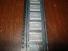
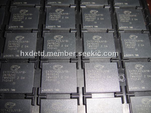
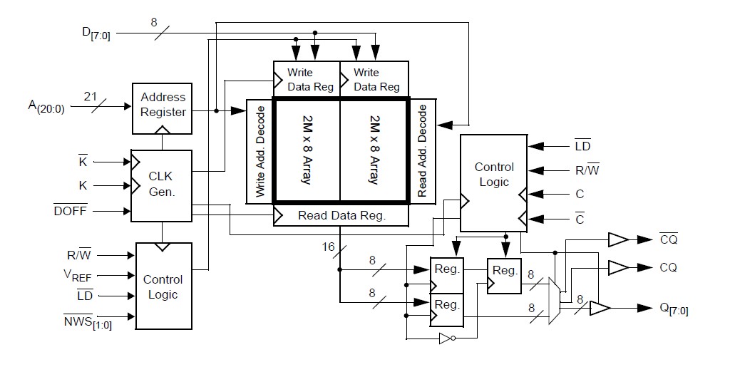
The CY7C1423JV18-267BZXC is a 1.8V Synchronous Pipelined SRAM, equipped with Double Data Rate Separate I/O (DDR-II SIO) architecture. The DDR-II SIO consists of two separate ports: the read port and the write port to access the memory array. The read port of the CY7C1423JV18-267BZXC has data outputs to support read operations and the write port has data inputs to support write operations.
Parametrics
CY7C1423JV18-267BZXC absolute maximum ratings: (1)Storage Temperature: –65℃ to +150℃; (2)Ambient Temperature with Power Applied: –55℃ to +125℃; (3)Supply Voltage on VDD Relative to GND: –0.5V to +2.9V; (4)Supply Voltage on VDDQ Relative to GND: –0.5V to +VDD; (5)DC Applied to Outputs in High-Z: –0.5V to VDDQ + 0.3V; (6)DC Input Voltage: –0.5V to VDD + 0.3V; (7)Current into Outputs (LOW): 20 mA; (8)Static Discharge Voltage (MIL-STD-883, M. 3015) > 2001V; (9)Latch-up Current > 200 mA.
Features
CY7C1423JV18-267BZXC features: (1)36 Mbit density (4M x 8, 4M x 9, 2M x 18, 1M x 36); (2)300 MHz clock for high bandwidth; (3)2-word burst for reducing address bus frequency; (4)Double Data Rate (DDR) interfaces (data transferred at 600 MHz) at 300 MHz; (5)Two input clocks (K and K) for precise DDR timing. SRAM uses rising edges only; (6)Two input clocks for output data (C and C) to minimize clock skew and flight time mismatches; (7)Echo clocks (CQ and CQ) simplify data capture in high speed systems; (8)Synchronous internally self-timed writes; (9)1.8V core power supply with HSTL inputs and outputs; (10)Variable drive HSTL output buffers.
Diagrams
| Image | Part No | Mfg | Description |  |
Pricing (USD) |
Quantity | ||||
|---|---|---|---|---|---|---|---|---|---|---|
 |
 CY7C1423JV18-267BZXC |
Cypress Semiconductor |
SRAM 2Mx18 1.8V DDR-II SIO BURST 2 SRAM |
Data Sheet |
Negotiable |
|
||||
|
CY7C1423JV18-267BZXCT |
Cypress Semiconductor |
SRAM 2Mx18 1.8V DDR-II Burst 2 SRAM |
Data Sheet |
Negotiable |
|
||||