(China (Mainland))

Product Summary
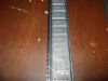
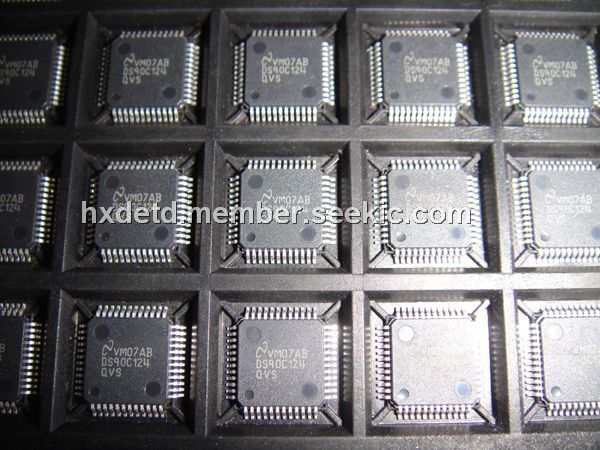
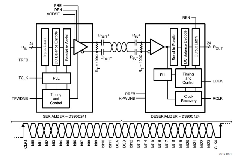
The DS90C124QVS is a 5-35MHz DC-balanced 24-bit FPD-Link II serializer/deserializer. The DS90C124QVS Chipset translates a 24-bit parallel bus into a fully transparent data/control LVDS serial stream with embedded clock information. This single serial stream simplifies transferring a 24-bit bus over PCB traces and cable by eliminating the skew problems between parallel data and clock paths. The DS90C124QVS saves system cost by narrowing data paths that in turn reduce PCB layers, cable width, and connector size and pins.
Parametrics
DS90C124QVS absolute maximum ratings: (1)Supply Voltage (VCC): -0.3V to +4V; (2)LVCMOS/LVTTL Input Voltage: -0.3V to (VCC +0.3V); (3)LVCMOS/LVTTL Output Voltage: -0.3V to (VCC +0.3V); (4)LVDS Receiver Input Voltage: -0.3V to 3.9V; (5)LVDS Driver Output Voltage: -0.3V to 3.9V; (6)LVDS Output Short Circuit Duration: 10 ms; (7)Junction Temperature: +150℃; (8)Storage Temperature: -65℃ to +150℃; (9)Lead Temperature(Soldering, 4 seconds): +260℃; (10)Maximum Package Power Dissipation Capacity Package De-rating: 48L TQFP 1/θJA ℃/W above +25℃.
Features
DS90C124QVS features: (1)User selectable clock edge for parallel data on both Transmitter and Receiver; (2)Internal DC Balancing encode/decode – Supports ACcoupling interface with no external coding required; (3)Individual power-down controls for both Transmitter and Receiver; (4)Embedded clock CDR (clock and data recovery) on Receiver and no external source of reference clock needed; (5)All codes RDL (random data lock) to support livepluggable applications; (6)LOCK output flag to ensure data integrity at Receiver side.
Diagrams
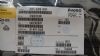
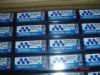
| Image | Part No | Mfg | Description |  |
Pricing (USD) |
Quantity | ||||||||||||
|---|---|---|---|---|---|---|---|---|---|---|---|---|---|---|---|---|---|---|
 |
 DS90C124QVS/NOPB |
National Semiconductor (TI) |
LVDS Interface IC |
Data Sheet |
|
|
||||||||||||
|
DS90C124QVSX/NOPB |
National Semiconductor (TI) |
LVDS Interface IC |
Data Sheet |
|
|
||||||||||||